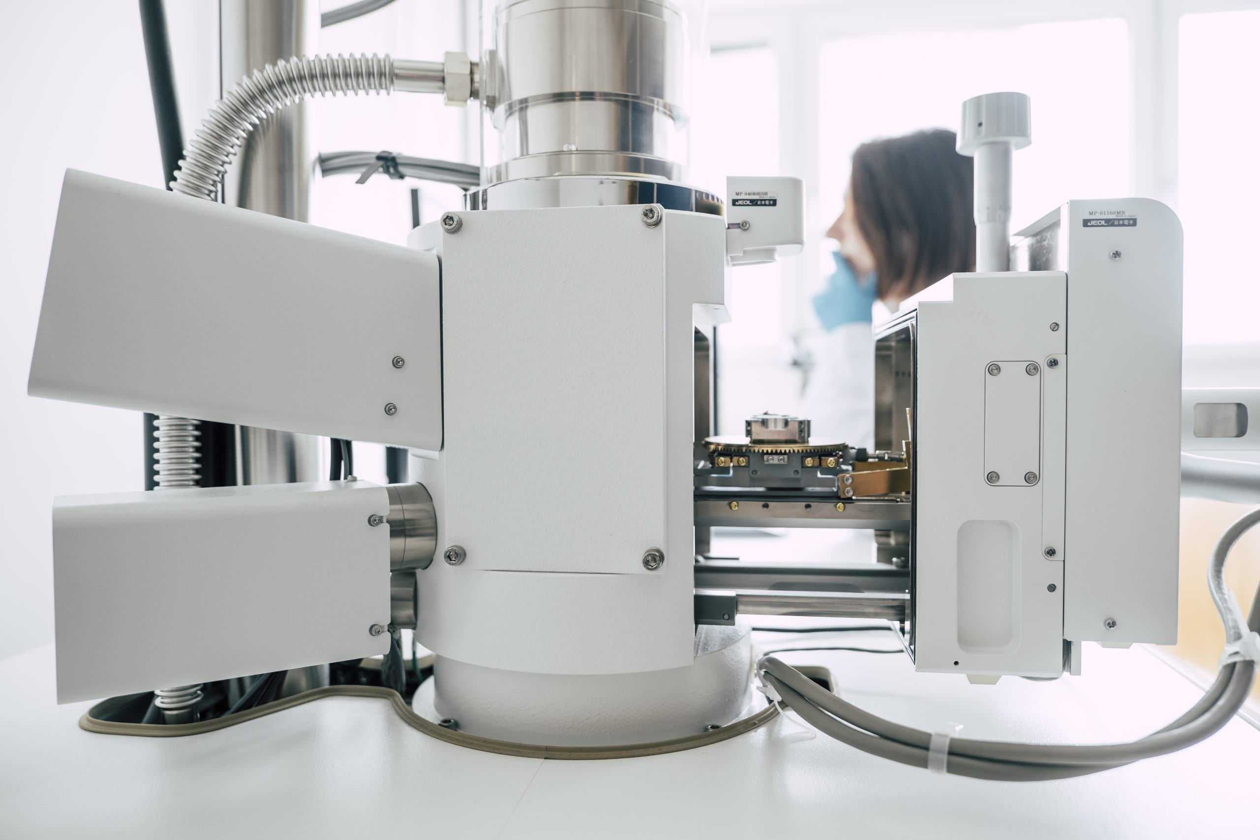
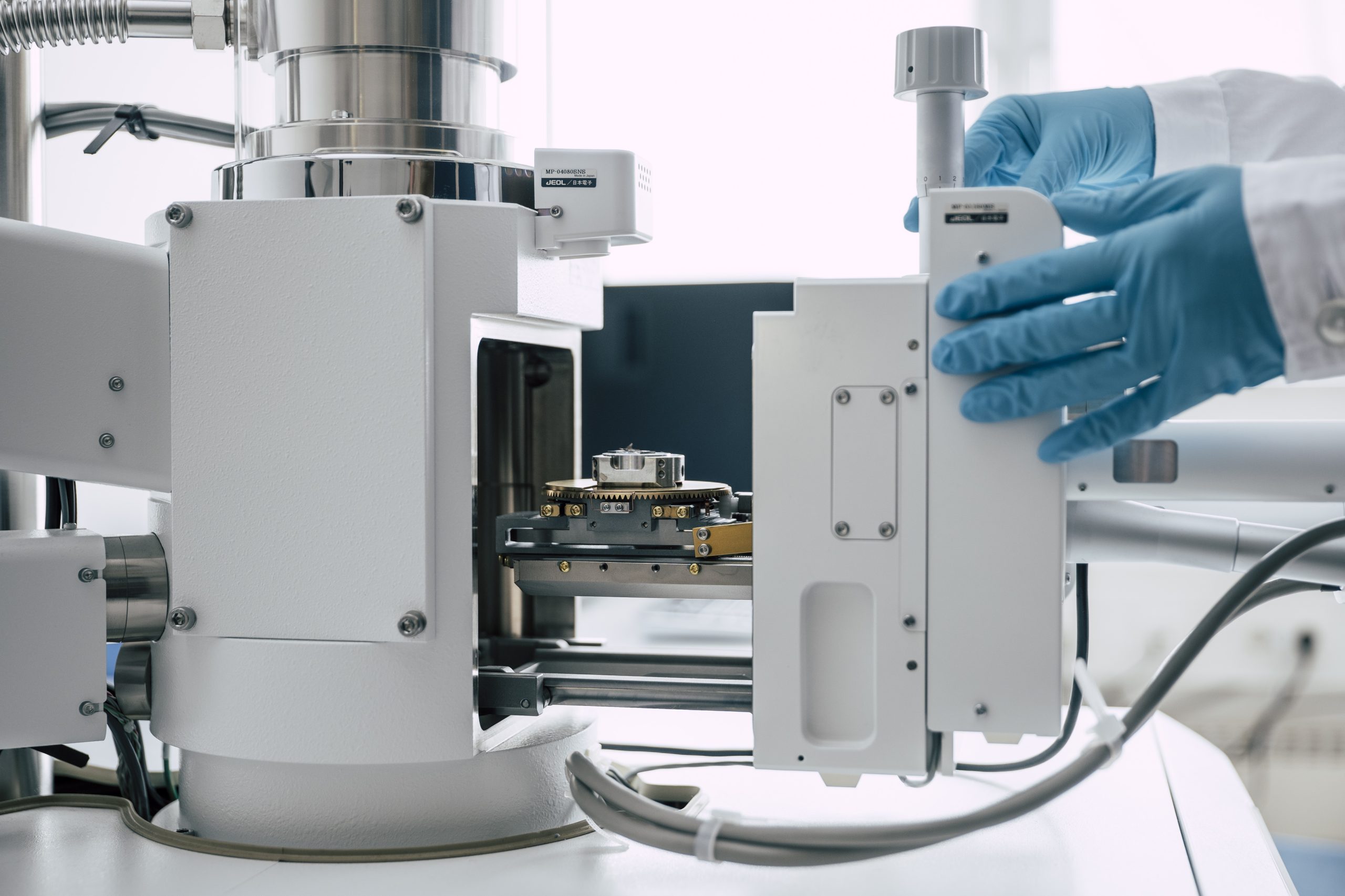
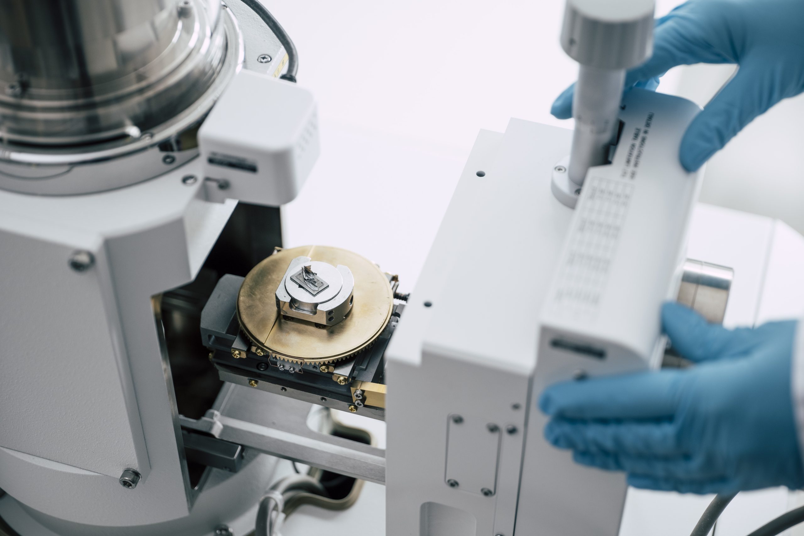
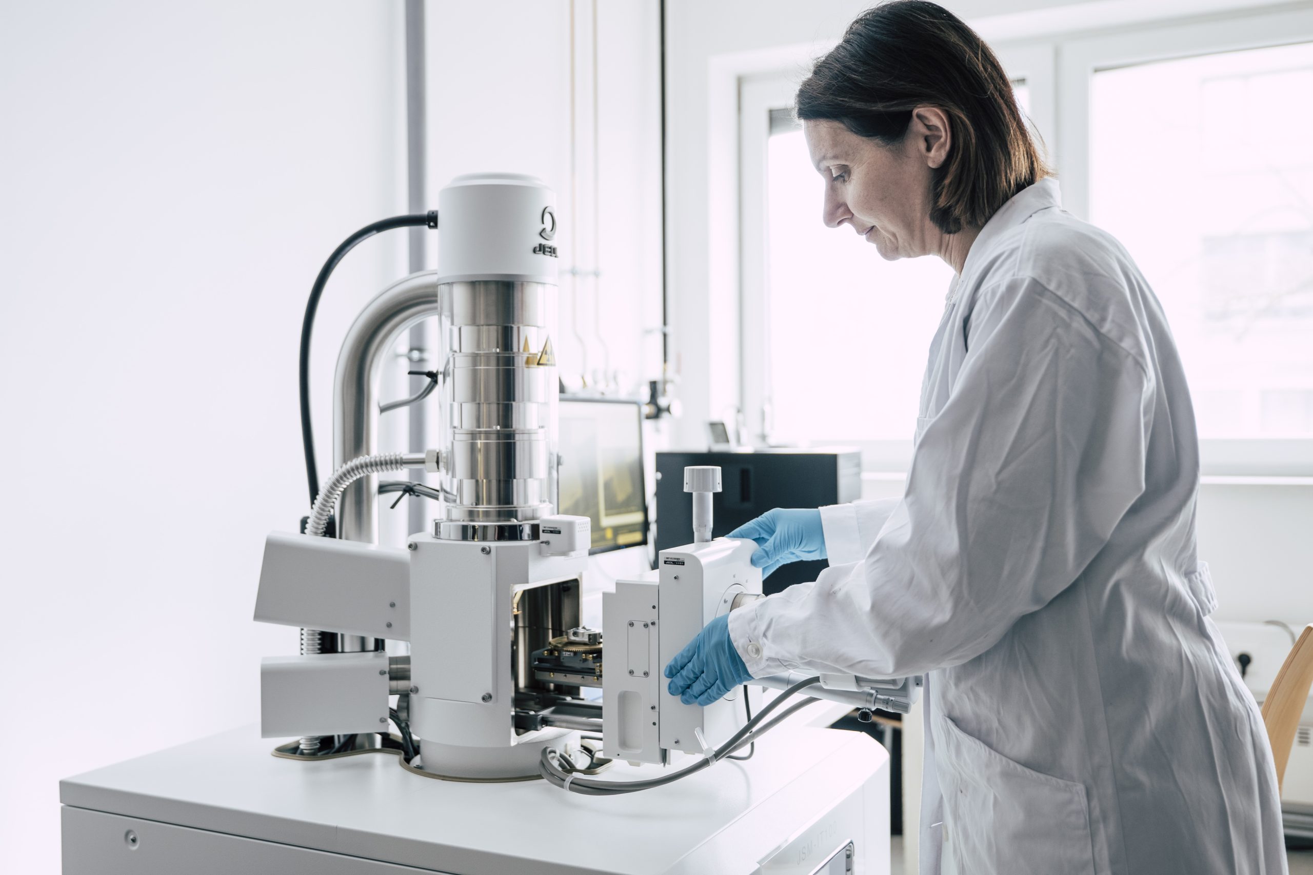
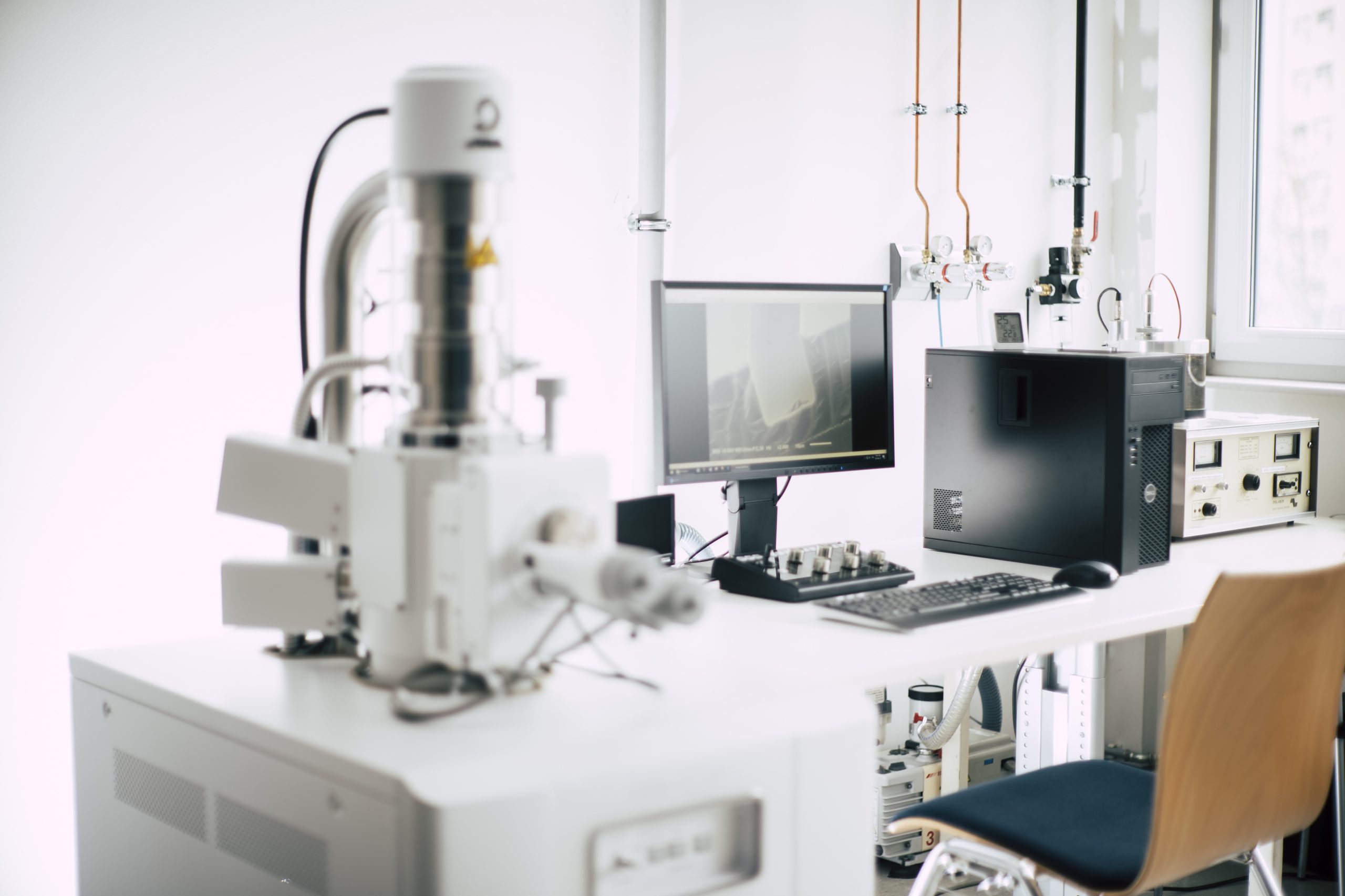
Scanning Electron Microscope (SEM) with EDS for high-resolution imaging and chemical element analysis of multilayer structures.
Equipment
JSM-IT 100 / JEOL
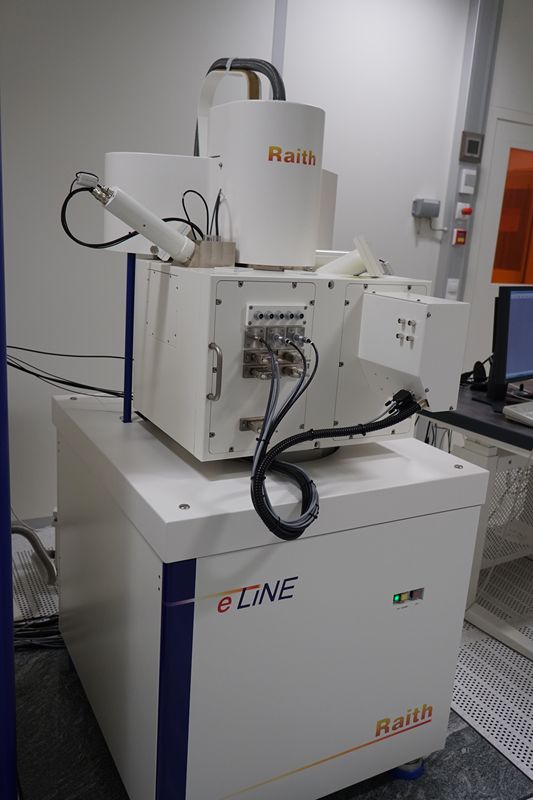
e-line / RAITH
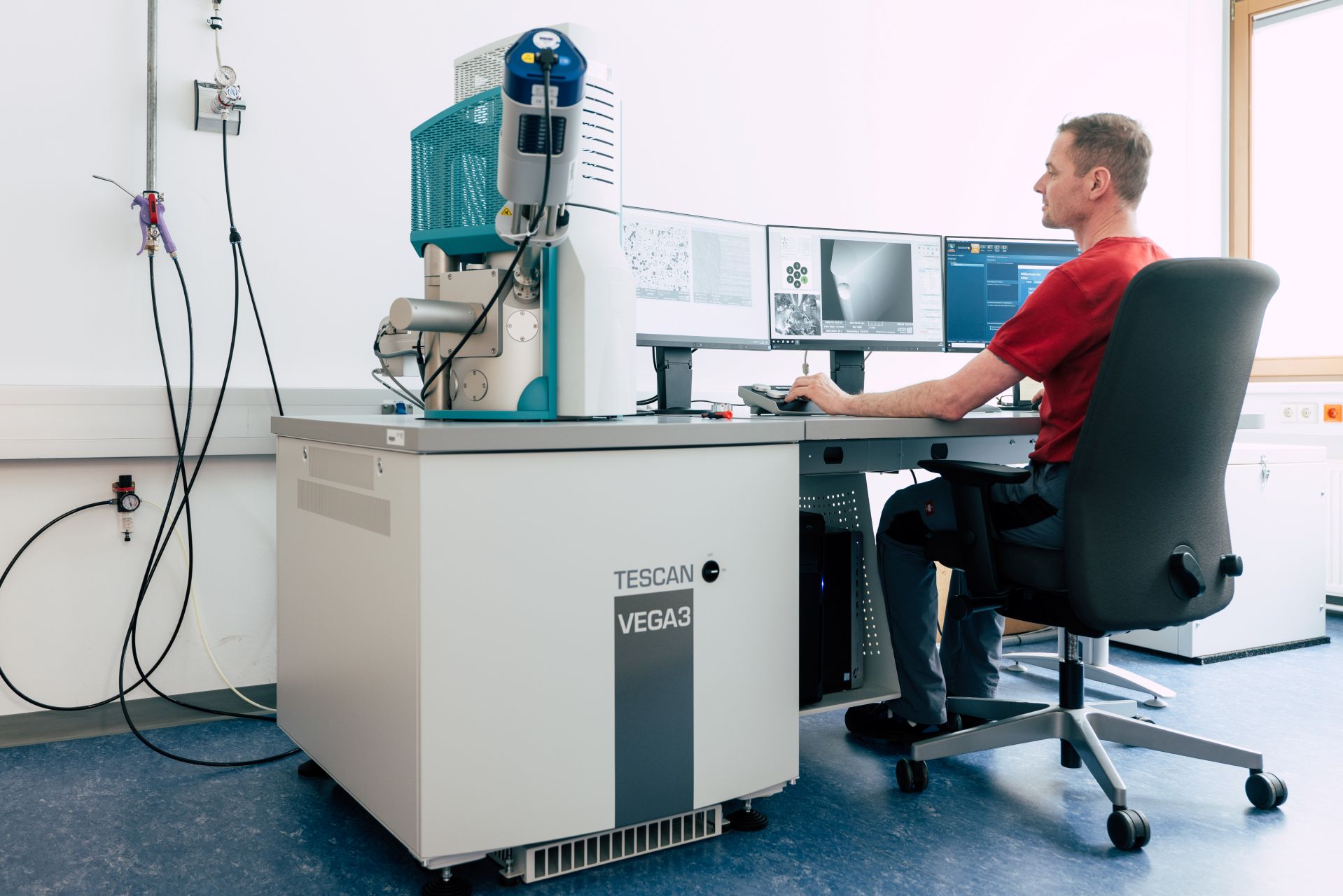
Vega 3 / TESCAN
Method
High-resolution imaging with the options of chemical element analysis by energy dispersive X-ray spectroscopy (EDS) and electron beam (e-beam) lithography (EBL).
Expected Result
High resolution images of the nanostructure, particles and surfaces. EDS option: enables precise analysis of chemical properties, essential for understanding material composition and arrangement. EBL option: Fabrication of structured surfaces from nm – µm dimensions.
Case Study
A customer in material science requires detailed imaging and compositional analysis of a multilayer metal coating. The SEM captures high-resolution images of each layer’s topography, while EDS detects the elemental composition, revealing differences in the distribution of metals across the layers.
Scanning Electron Microscope SEM JSM-IT 100 / JEOL
Specifications
Maximum sample size: diameter 80 mm, height 35 mm
Sample loading and unloading time: ≤ 4 minutes
Resolution: nominal (diam. e-beam) 4 nm, in practice features down to ≈100nm resolved (reasonable magnification x30.000 at 128 mm x 96 mm image), depends heavily on sample. Requests of customers are checked individually.
Accelerating Voltage: 0.5 to 20 kV
Sample manipulation (stage): tilt -10° to 90° ; rotation 360° ; movement: 80 x 40 mm
Low vacuum option for non-conductive / out-gassing samples
Vega 3 SEM + AZtec Energy-Dispersive X-ray Spectroscopy (EDX)
Specifications
OXFORD INSTRUMENTS AZtec energy dispersive X-ray spectroscopy detector (EDX)
Heated tungsten filament cathode
Wide Field Optics™ Technology with Intermediate Lens™ and In-Flight Beam Tracing™
Resolution:
High Vacuum Mode: 3 nm at 30 keV. 8 nm at 3 keV
Low Vacuum Mode: 3.5 nm at 30 keV with BSE detector
Maximum Field of View: >50 mm at max WD
Chemical element analysis by EDS (~0.1 wt.-% for sodium and heavier elements)
Scanning Electron Microscope SEM e-line / RAITH
Specifications
Max. sample size: 100 mm × 100 mm (4” wafer) on flat sample holder, 20 mm × 20 mm on tiltable / rotatable stage
Max. sample height: 20 mm
Max. acceleration voltage: 30 kV
Resolution: < 5 nm
Sample manipulation (RT stage): tilt up to 92° ; rotation 360°
Emitter type: Thermionic (tungsten emitter)
Surface needs intrinsic conductivity or will be coated (Au, W)
UV-Vis/NIR spectrometer for analyzing transmission, reflection, and absorption of solid and liquid samples. Ideal for optical material characterization in research and development.
The tensile testing machine enables precise measurement of tensile strength, elongation and modulus of elasticity of a wide range of materials in research, development and quality control.