


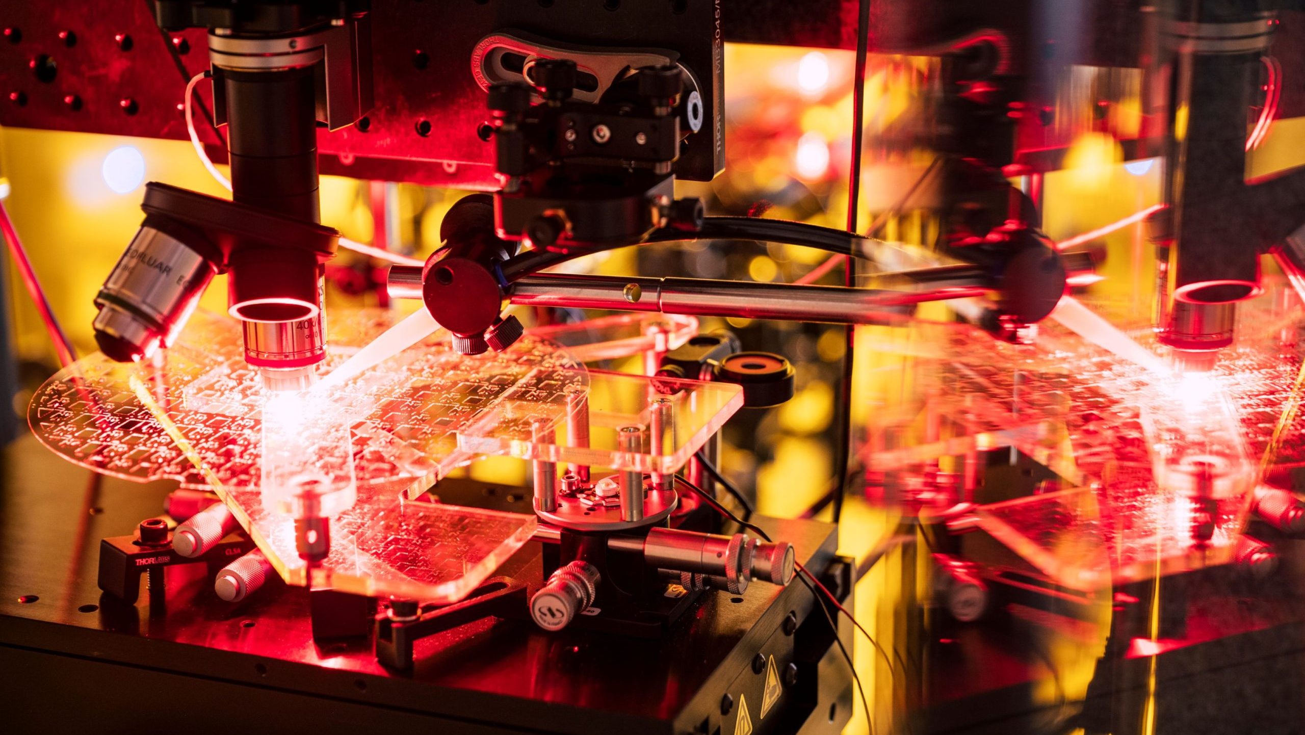
Photonic circuits are tiny components that operate using light. Researchers at our MATERIALS Institute are fabricating such circuits directly in glass. To do this, they use femtosecond lasers: extremely short laser pulses that alter the material only at precisely defined points. This creates fine pathways that can guide light through the chip, split it and recombine it.
The current study was published in the journal *Photonics*. It details key developments from the four FFG projects OptoQuant, FLMOptChips, PIQLearn and ScaleQUDITS.
Using light to trace delicate patterns on glass
At the MATERIALS Institute, we cover the entire development process: from computer-aided design through laser processing to the testing of the finished components. As the structures are written directly onto the glass, new ideas can be tested quickly and adapted to different applications.
For this latest work, the team integrated optical pathways, three-dimensional glass structures and electric heating elements into a single glass chip. The rapid and flexible manufacturing process is particularly well suited to prototypes and small production runs.
A tiny glass bridge saves energy
At the heart of the chip is a cantilevered microbridge made of glass. A light path and a small electric heating element run through it. When the bridge is heated, the propagation of the light changes. As virtually no heat is lost to the rest of the glass in the process, the light can be controlled with minimal energy consumption.
The component requires around 17 milliwatts of electrical power across the entire intended control range. The results thus demonstrate that controllable photonic circuits can be realised in glass in this way.
New possibilities for compact glass chips
The approach developed combines light guidance, control and electrical connectivity in a single component. This enables compact photonic chips to be developed more quickly and tailored specifically to different tasks. Three-dimensional light paths offer additional design flexibility. Potential applications range from compact measurement systems and optical data processing to quantum technology.
This publication marks the conclusion of four successful FFG projects. The technology developed as part of these projects expands the manufacturing capabilities of the MATERIALS Institute and lays the foundations for compact, customisable photonic components with low energy consumption.
Publication
Philip Lichtenegger, Philipp Hurdax, Georg Spernbauer and Bernhard Lamprecht:
„Reconfigurable Photonic Integrated Circuits in Glass by Femtosecond Laser Writing and Laser-Induced Chemical Etching“, Photonics 2026, 13(8), 731.