- About us
- Research fields
- DIGITAL – Institut für Digitale Technologien
- MATERIALS – Institut für Sensorik, Photonik und Fertigungstechnologien
- ROBOTICS – Institut für Robotik und Flexible Produktion
- COREMED – Zentrum für Regenerative Medizin und Präzisionsmedizin
- HEALTH – Institut für Biomedizinische Forschung und Technologien
- LIFE – Institut für Klima, Energiesysteme und Gesellschaft
- POLICIES – Institut für Wirtschafts-, Sozial und Innovationsforschung
- Business areas
- Products & services
- Research infrastructure
- Beteiligungen
- Career
- Aktuelles
- Publications
- Kontakt zu uns


Microassembly Lab
Microassembly Lab for photonic and electronic assemblies
Chip Bonding Plattform, Foto: JOANNEUM RESEARCH/Schwarzl
What does the Microassembly Lab for photonic and electronic assemblies offer?
Design and production of optoelectronic components and devices from micrometre scale to (hybrid) macroscopic assemblies
- Electronic design
EDA software Altium Designer for analogue and digital circuit design, including SPICE simulation; Xilinx and Intel PSG (Altera) design environment for FPGA and CPLD; micro-controller programming (e.g. with ARM KEILTools) - Data and signal analysis
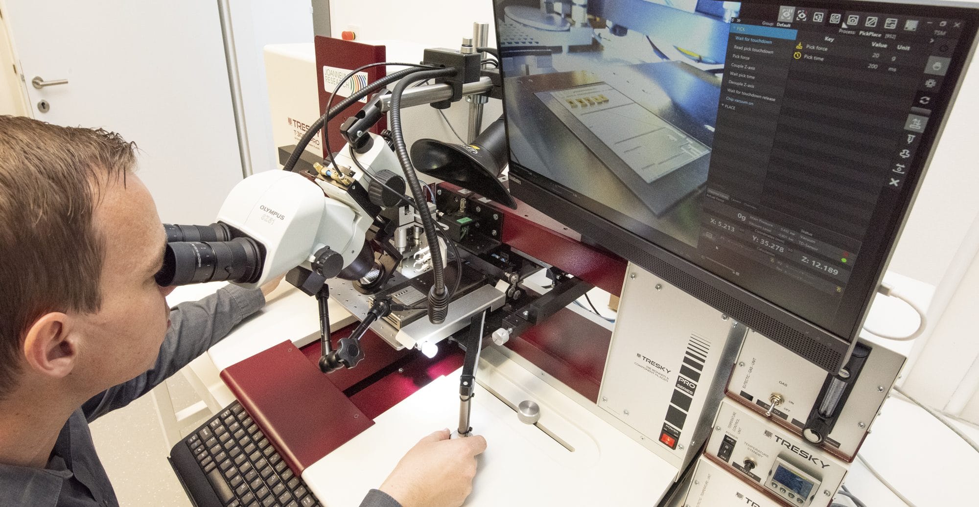
MATLAB, GNU Octave and Simulink/Simscape; algorithm development and system modelling. - Chip bonding platform
This high-precision Tresky platform is capable of placing and bonding electronic components on surfaces with more than 10µ accuracy. The Tresky Chip Bonder features True Vertical Technology™, which guarantees parallelism between chip and substrate. - SMD placement
Neoden 4 pick & place machine - Soldering processes
Inert gas and forming gas reflow soldering up to 450° C (vacuum); vapour phase soldering system (oxygen-free reflow process); universal soldering and repair station (JBC).
Realisation of "Printed Electronics and Optics" through additive processes: Screen printing, inkjet printing/electrostatic inkjet printing (ESJet), aerosol jet printing and atmospheric pressure plasma jet processes.
- Atmospheric pressure plasmajet coating system
Atmospheric pressure plasmajet coating technologies (APPJ) do not require a vacuum chamber and are therefore subject to hardly any size restrictions with regard to the components to be coated. Possible applications include electrical insulation layers or conductor tracks and electrodes, etc. - Inkjet printers
Four modern inkjet printers are available, three PIXDRO LP50 platforms and a Dimatix DMP 2800 printing platform, which enable the use of the most important industrial print head types. - Optomec aerosol jet printers
Our aerosol jet printing process is a non-contact direct structuring process with high resolution (up to 10µm) and also enables the use of non-planar substrates and the creation of 2.5D structures. - ESJET printer
Electrostatic Jet Printing technology is used to apply functional inks in a viscosity range and droplet volume that is currently not available for conventional piezo-based inkjet technologies. - Solenoid valve printers
Compared to inkjet printing, this technology allows the application of larger drop volumes and working in a wider viscosity range with a larger minimum line width and lower possible printing frequency. - Flexographic printing
Highly viscous inks or pastes are applied to the ink application roller via a doctor blade, which then wets the prefabricated cliché with the structures to be transferred. In the roller-based process, the ink is then transferred from the cliché to the substrate to be printed. - Thieme precision screen printing machine
In screen printing, a highly viscous ink or paste is applied to the substrate via a pre-structured screen (stencil) using a doctor blade. Parameters such as squeegee speed, mesh fineness and mesh size of the screen determine the printing result.

Your contact
Location
Das sagen unsere Kunden
Further research infrastructure
Certified class 6 cleanroom for nanostructures and innovative electronic components and sensors
This highly precise maskless laser system (MALA) is suitable for the production of highly complex and stepless micro-optical structures.
The lab includes flexible, rapid prototyping processes to produce a variety of structures in a wide range of materials.
We offer laser material processing and many years of expertise in materials science.
State-of-the-art development infrastructure for integrated electronic and optical design including EMC and ESD - open to industrial partners.
Our R2R-UV-NIL pilot line enables the continuous and cost-effective production of micro and nanostructures on flexible large-area film substrates for applications in lighting, photovoltaics, AR/VR, AR/VR, microfluidics, diagnostics, security, film finishing and packaging, the pharmaceutical industry and life sciences.
State-of-the-art infrastructure for light measurement and prototype production for integrated optical and electronic design - open to industrial partners.
Our laboratory includes technologies for functional plasma coating at low temperatures from atmospheric pressure to fine and high vacuum.
Printing technologies for the development of customised 2D, 2.5D and 3D printing processes
Measurement and analysis of the smallest structures, layers and components on a micro- and nanometre scale on various substrates (including flexible ones)
We use a specially modified EVG770 Nanoimprint Lithography (NIL) stepper for the large-scale production of micro- and nanostructures in UV imprint resins. Together with special materials and processes, we achieve the highest precision right down to practically seamless transitions between individual structures.
SHAPING THE FUTURE, TOGETHER
JOANNEUM RESEARCH provides innovation and technology services in the field of applied research. As a research company working on behalf of various federal provinces and regions in Austria, our expertise shapes the development of our modern society and economy – sustainably, and always with a focus on people. As a multidisciplinary team working in a flexible set-up that fosters innovation, we always live up to the highest social and scientific standards.