Institute for Sensors, Photonics and Manufacturing Technologies
Research groups
Products & services
Environmental, bioanalytical and diagnostic sensor technology combined with smart microfluidic lab-on-a-chip and organ-on-a-chip systems
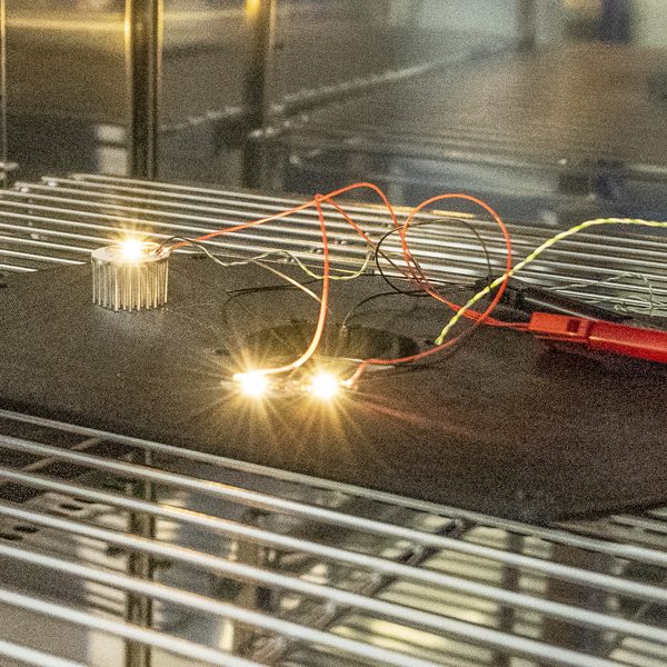
Cost-effective solutions by extending the functions of classic LED-based lighting systems in the areas of Visible Light Communication, Visible Light Positioning and Visible Light Sensing
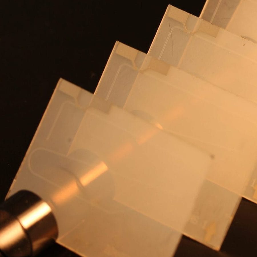
R2R-UV-NIL pilot line for the continuous and cost-effective production of micro- and nanostructures on flexible large-area film substrates
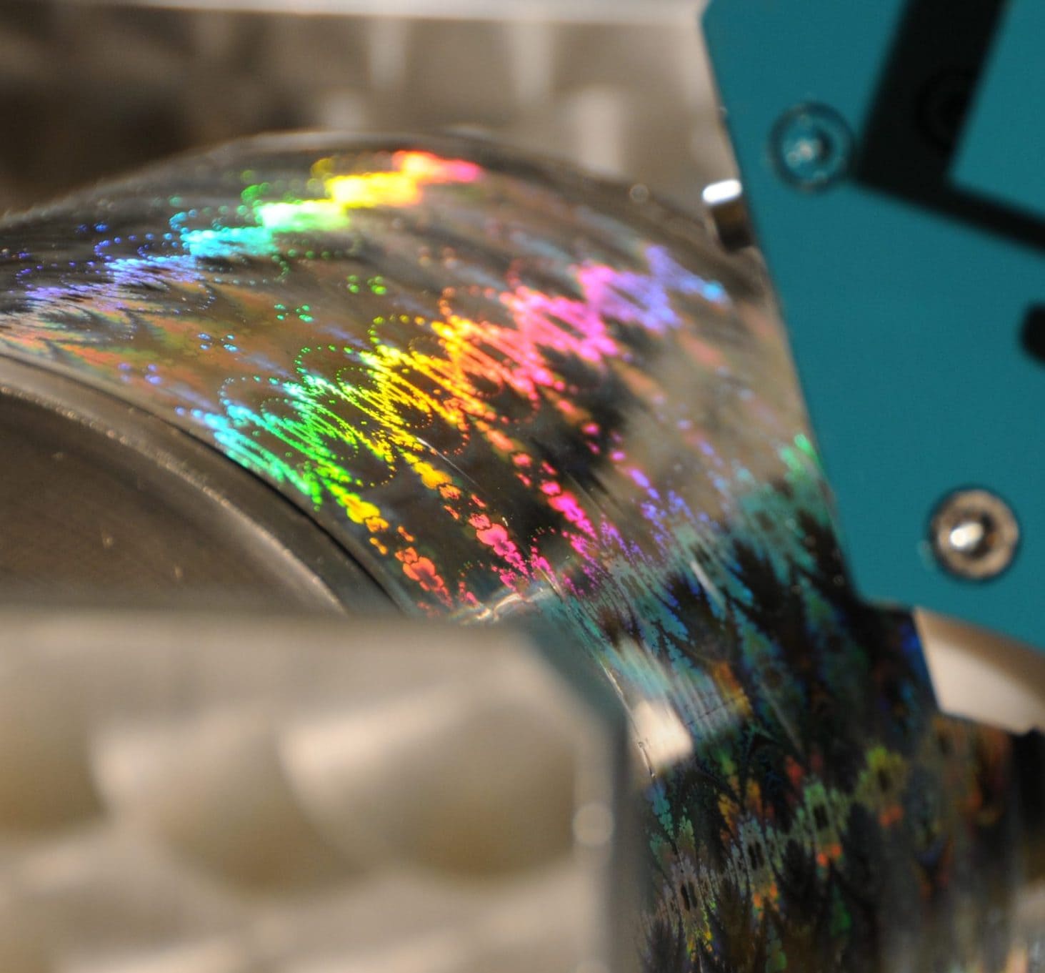
Complete solutions from optical simulation, mastering and prototyping to the transition to high volume, cost effective production of optical structures and components
Reusable materials, components and compounds and their applications, e,g, coatings developed in-house for UV imprint lithography (NILcure®)
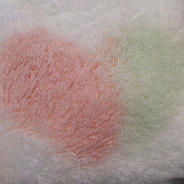
Innovative, covalently bonded pH indicator dyes for smart materials – visible in colour change, durable and versatile.
Printable sensor inks and sensors with piezoelectric, pyroelectric and magnetoelectric features
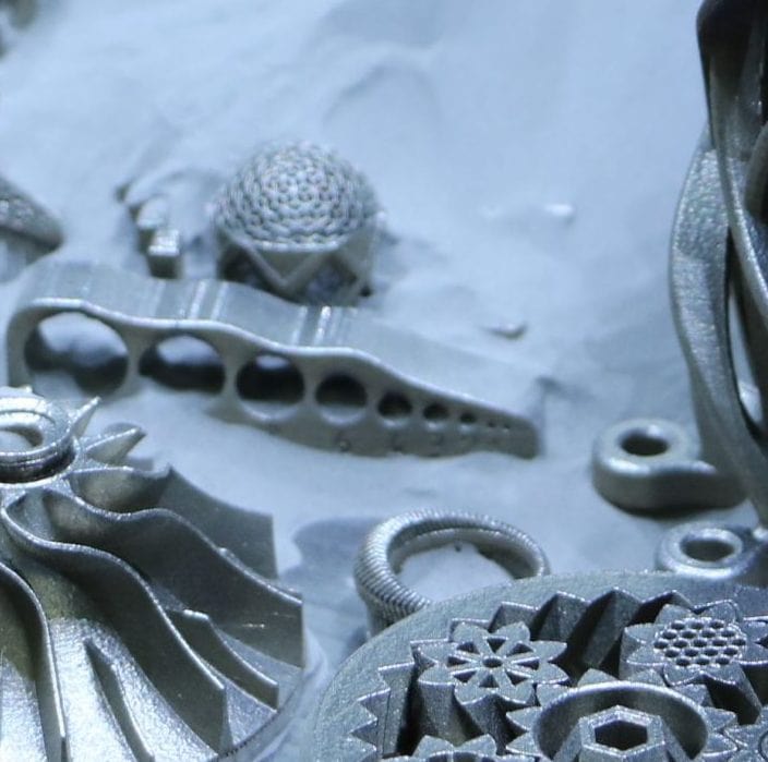
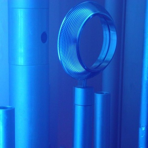
Additive manufacturing thanks to new design and simulation tools, new materials and the realisation of special topological structures
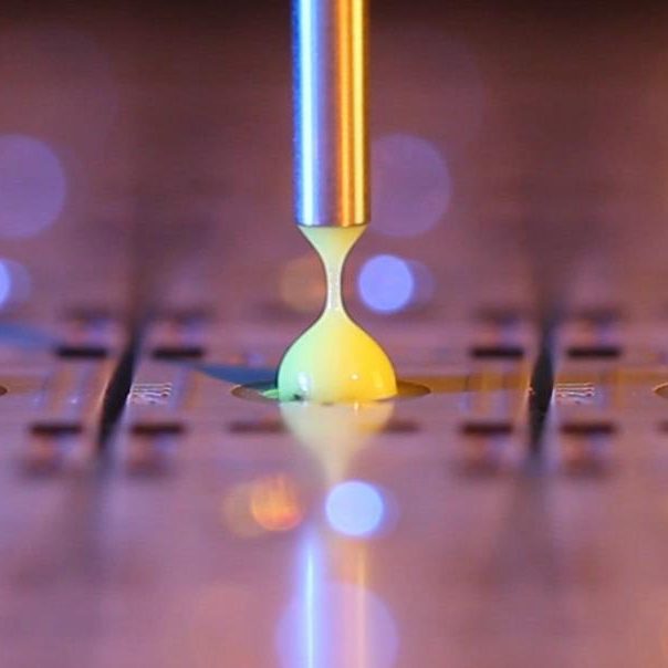
Ultrashort laser pulses to directly write 3D microstructures in a variety of different materials
Functional coating processes: Plasma and vacuum coating (PVD, PA-CVD), atmospheric pressure plasma coating processes as well as digital printing processes
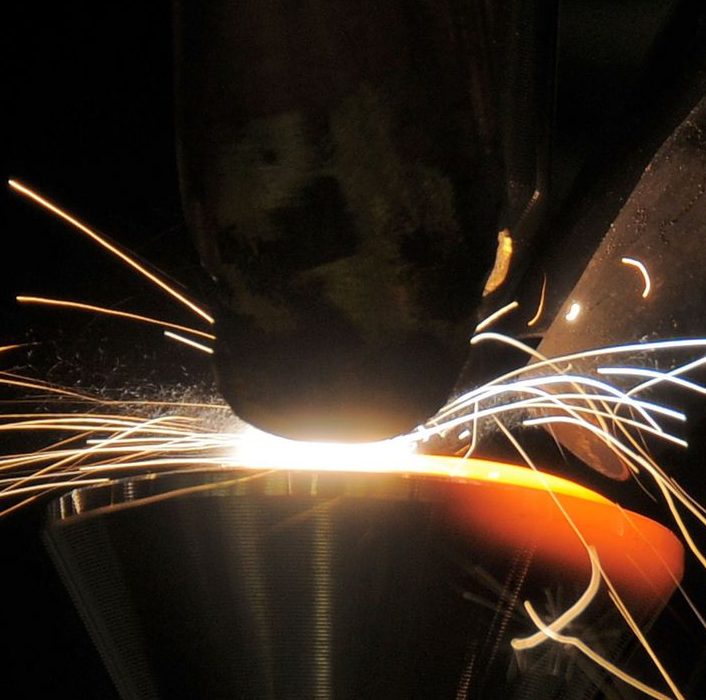
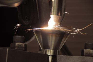
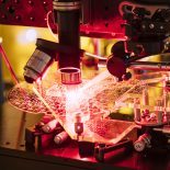
Laser welding, laser alloying and laser cladding, with a particular focus on materials expertise
Research infrastructure
Measurement and analysis of the smallest structures, layers and components on a micro- and nanometre scale on various substrates (including flexible ones)
We use a specially modified EVG770 Nanoimprint Lithography (NIL) stepper for the large-scale production of micro- and nanostructures in UV imprint resins. Together with special materials and processes, we achieve the highest precision right down to practically seamless transitions between individual structures.
Certified class 6 cleanroom for nanostructures and innovative electronic components and sensors
Microassembly Lab for photonic and electronic assemblies
This highly precise maskless laser system (MALA) is suitable for the production of highly complex and stepless micro-optical structures.
The lab includes flexible, rapid prototyping processes to produce a variety of structures in a wide range of materials.
We offer laser material processing and many years of expertise in materials science.
State-of-the-art development infrastructure for integrated electronic and optical design including EMC and ESD - open to industrial partners.
Our R2R-UV-NIL pilot line enables the continuous and cost-effective production of micro and nanostructures on flexible large-area film substrates for applications in lighting, photovoltaics, AR/VR, AR/VR, microfluidics, diagnostics, security, film finishing and packaging, the pharmaceutical industry and life sciences.
State-of-the-art infrastructure for light measurement and prototype production for integrated optical and electronic design - open to industrial partners.
Our laboratory includes technologies for functional plasma coating at low temperatures from atmospheric pressure to fine and high vacuum.
Printing technologies for the development of customised 2D, 2.5D and 3D printing processes
Projects
Business areas
News and events
Publications