

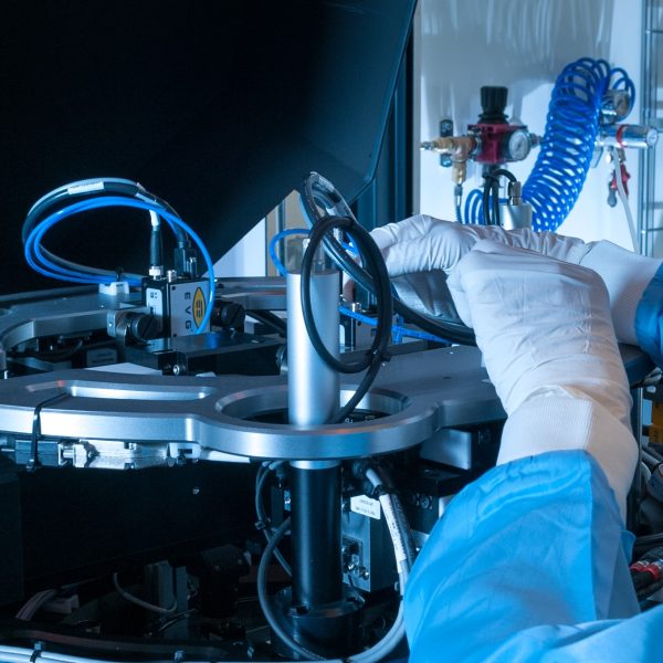
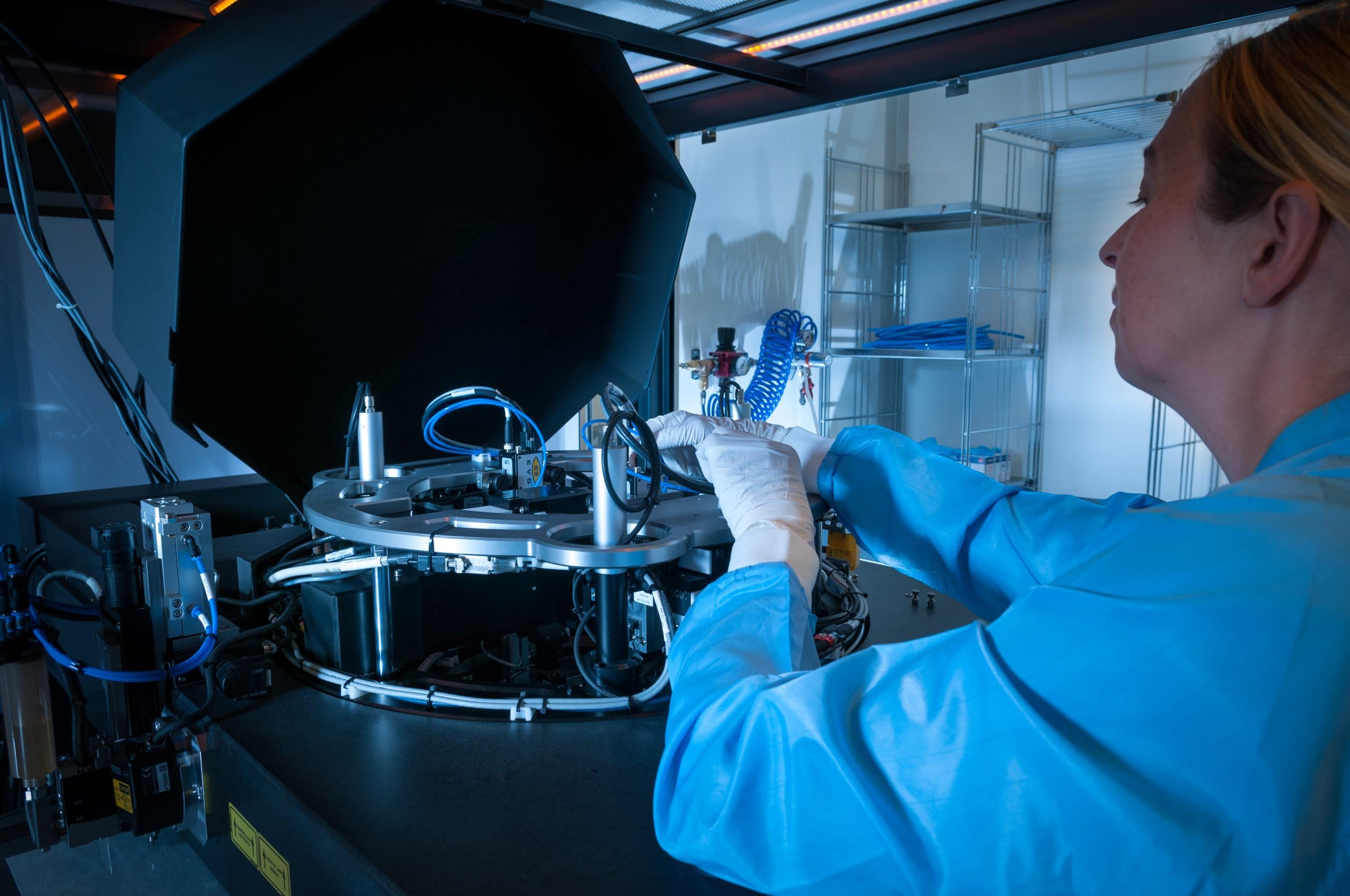
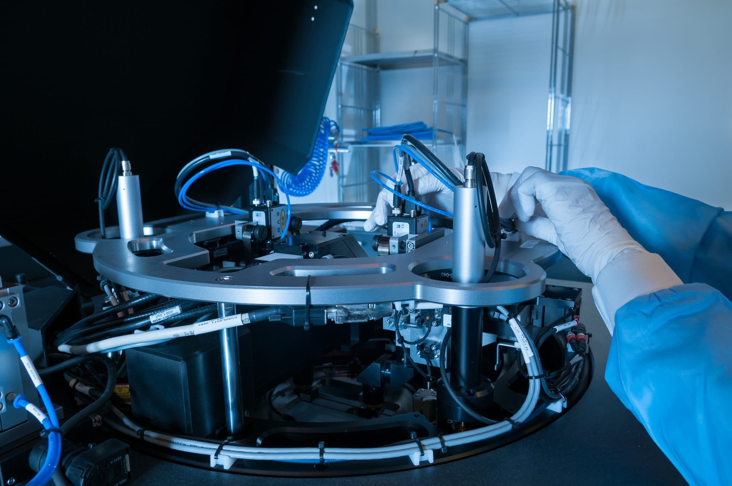

Environmental, bioanalytical and diagnostic sensor technology combined with smart microfluidic lab-on-a-chip and organ-on-a-chip systems
Printable sensor inks and sensors with piezoelectric, pyroelectric and magnetoelectric features
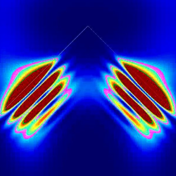
Cost-effective solutions by extending the functions of classic LED-based lighting systems in the areas of Visible Light Communication, Visible Light Positioning and Visible Light Sensing
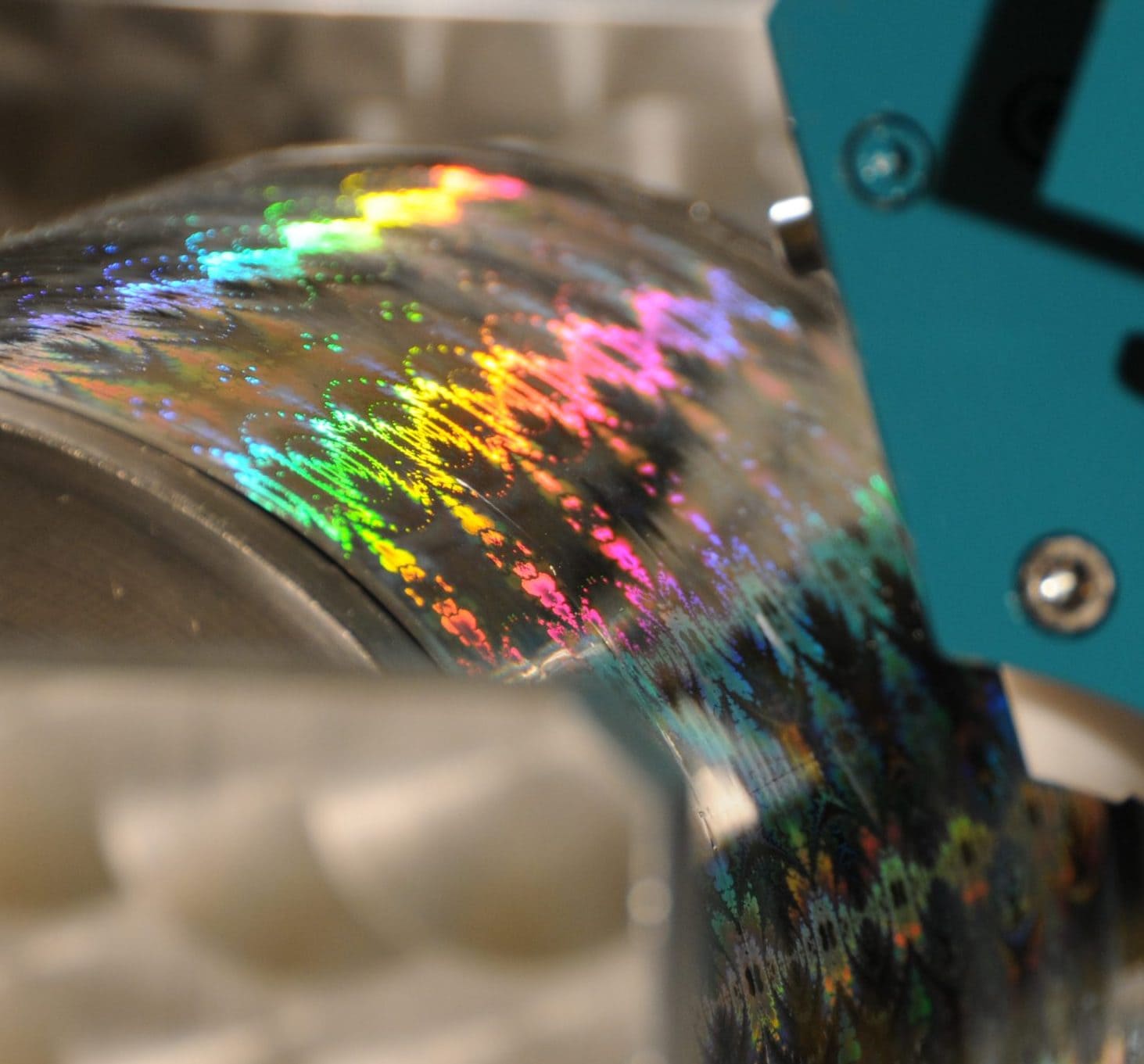
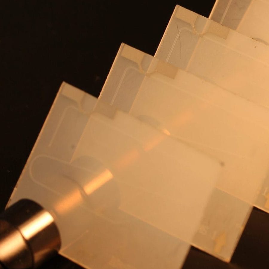
R2R-UV-NIL pilot line for the continuous and cost-effective production of micro- and nanostructures on flexible large-area film substrates
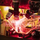
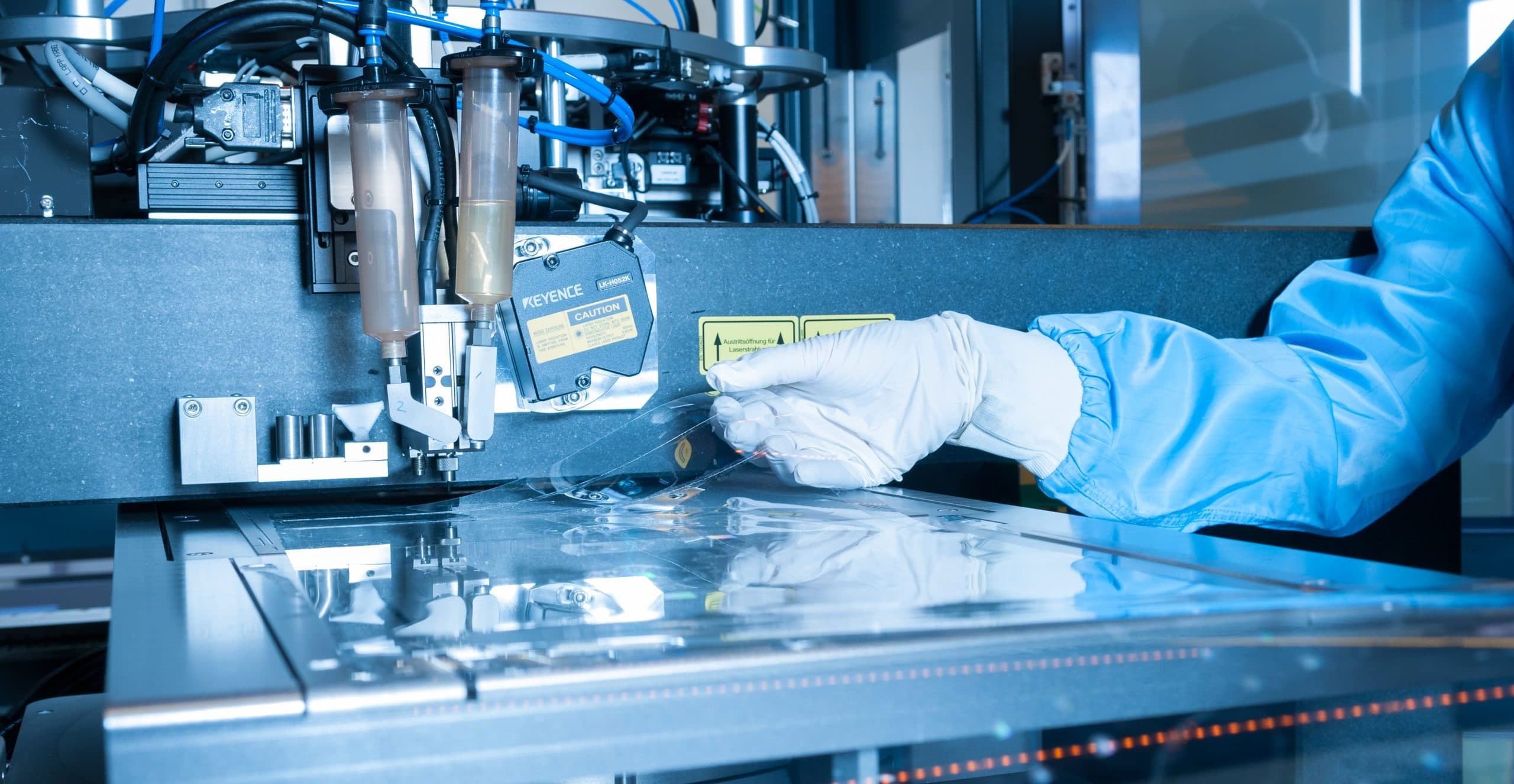
Ultrashort laser pulses to directly write 3D microstructures in a variety of different materials
Functional coating processes: Plasma and vacuum coating (PVD, PA-CVD), atmospheric pressure plasma coating processes as well as digital printing processes

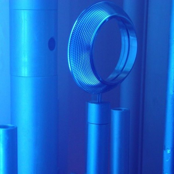
Laser welding, laser alloying and laser cladding, with a particular focus on materials expertise
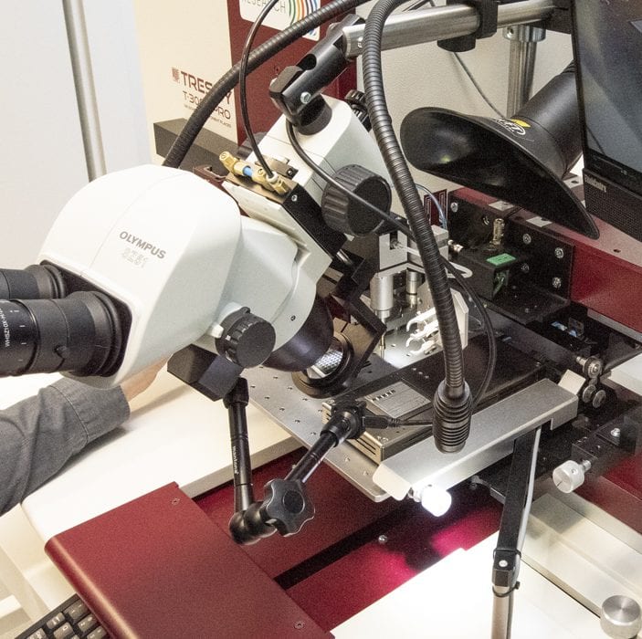
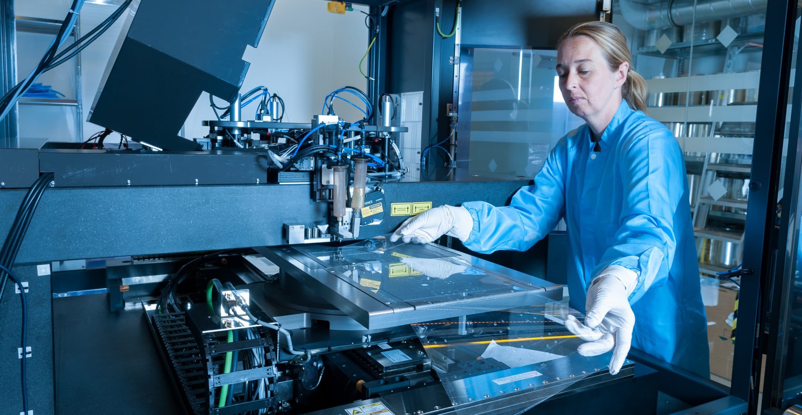
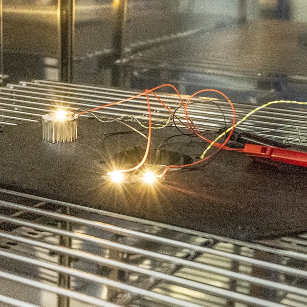
Development of customised prototypes, especially in the areas of LED lighting and sensor technology: circuit design, the conception of the system through to prototyping
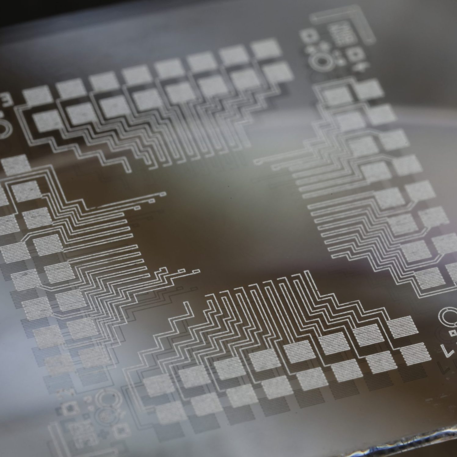
Scalable and digital printing processes (including 3D printing of electronics) for generative manufacturing of functional components
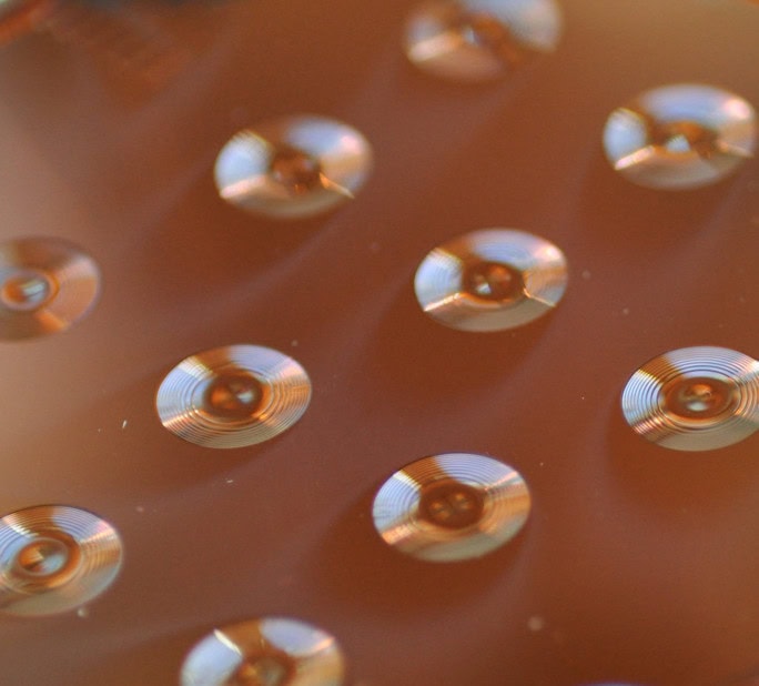
Overall concepts for design, simulation, optimisation and prototyping of optical components for customised lighting solutions
High-resolution 3D structuring using two-photon lithography, as well as 2D and continuous 2.5D structuring using maskless grayscale laser lithography and electron beam lithography