

Umwelt-, bioanalytische und diagnostische Sensorik kombiniert mit smarten mikrofluidischen Lab-on-a-Chip und Organ-on-a-Chip-Systemen
Printable sensor inks and sensors with piezoelectric, pyroelectric and magnetoelectric properties
We develop cost-effective solutions by extending the capabilities of classic LED-based lighting systems in visible light communication, visible light positioning and visible light sensing
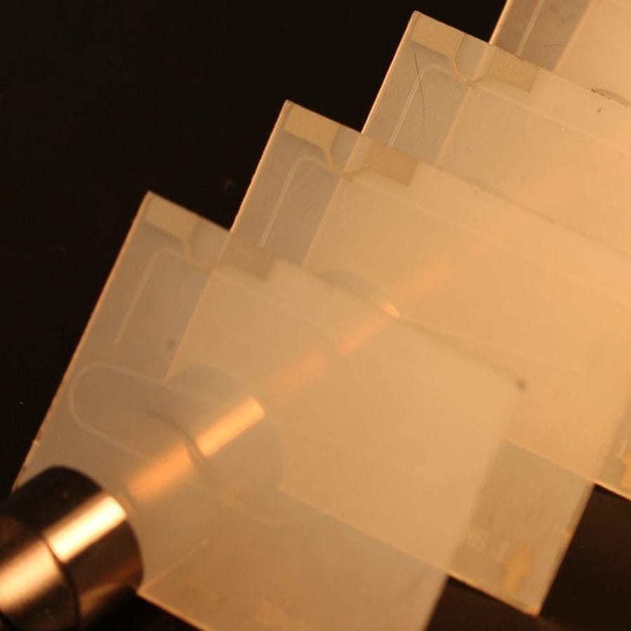
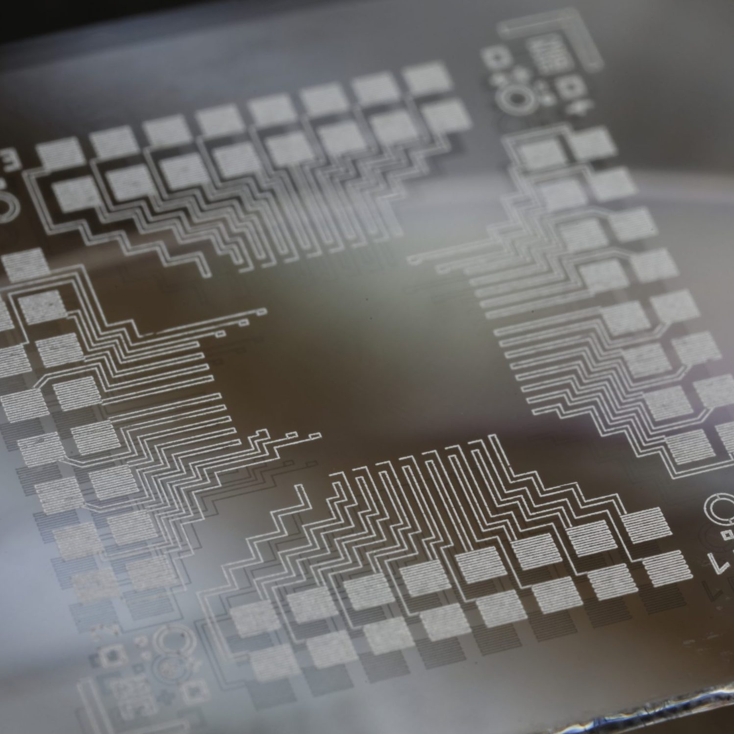
R2R-UV-NIL pilot line for the continuous and cost-effective production of micro- and nanostructures on flexible large-area film substrates
Replikation von Master-Strukturen nahezu nahtlos auf großer Fläche (bis zu 380 x 700 mm²) mittels Step&Repeat UV-NIL-Prozess
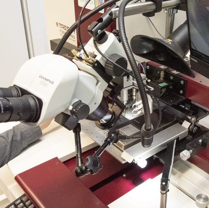
Messungen und Analyse von kleinsten Strukturen, Schichten und Bauelementen im Mikro- und Nanometermaßstab
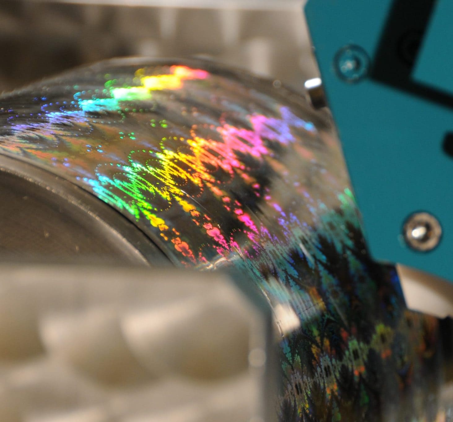
Complete solutions from optical simulation, mastering and prototyping to the transfer to large-scale, cost-efficient production of optical structures and components
Wiederverwendbare Materialien, Komponenten bzw. Verbundstoffe und deren Anwendungen, wie z.B. selbst entwickelte Lacke für die UV-Imprint-Lithografie (NILcure®)
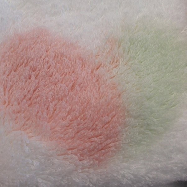
Innovative, kovalent gebundene pH-Indikatorfarbstoffe für smarte Materialien – sichtbar im Farbwechsel, langlebig und vielseitig einsetzbar.
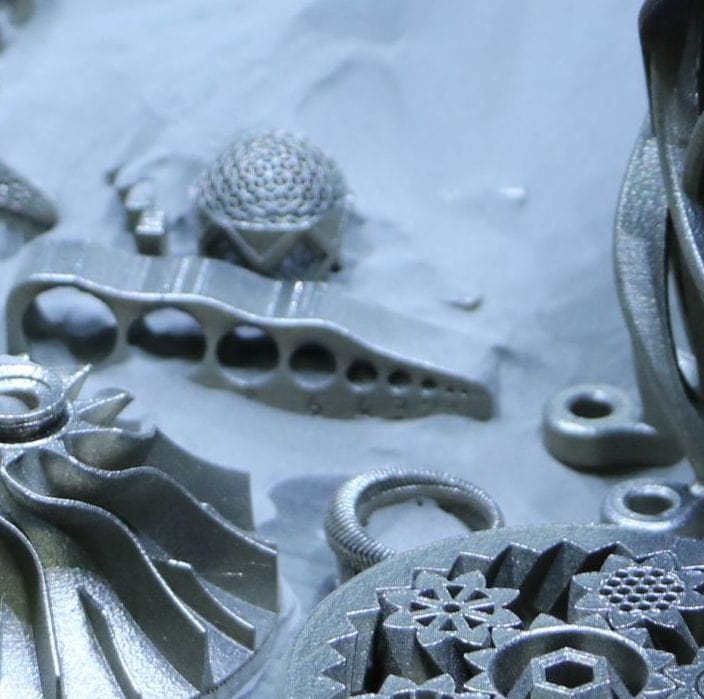
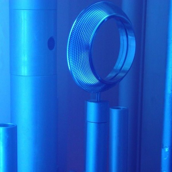
Additive Fertigung durch neu verfügbare Konstruktions- und Simulationswerkzeuge sowie durch neue Materialien und Realisierung spezieller Gitterstrukturen
Ultrakurze Laserpulse zur direkten Erzeugung von dreidimensionalen Mikrostrukturen in einer Vielzahl unterschiedlicher Materialien
Funktionelle Beschichtungsverfahren: Plasma- und Vakuumbeschichtung (PVD, PA-CVD), Atmosphärendruck-Plasmajetverfahren sowie auch digitale Druckverfahren
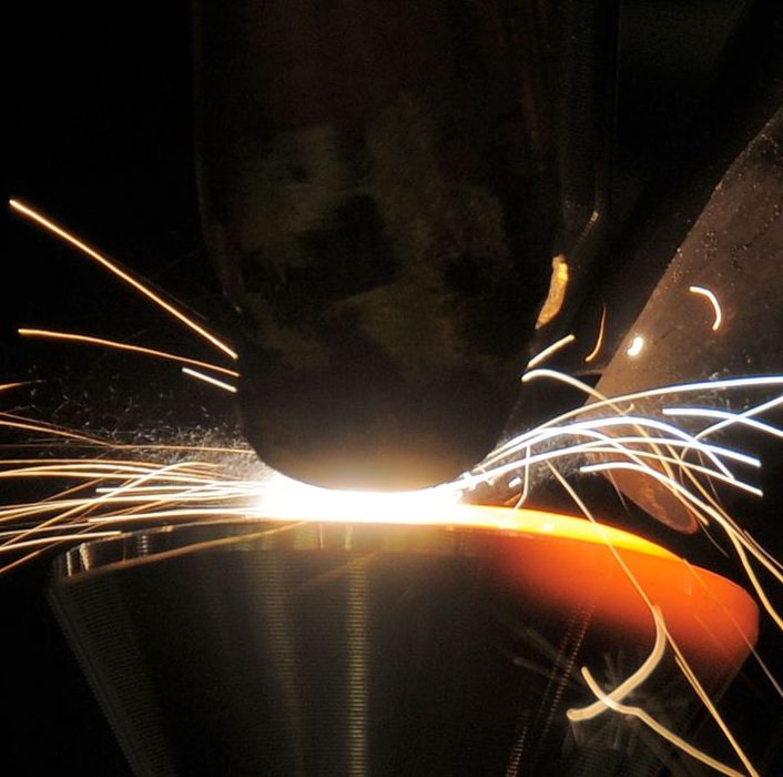
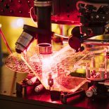
Laserschweißen, Laserlegieren und Laserauftragsschweißen, mit besonderem Schwerpunkt auf Werkstoffkompetenz
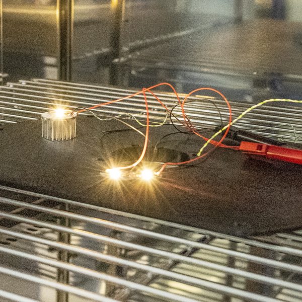
Development of customised prototypes, with a particular focus on LED lighting and sensor technology
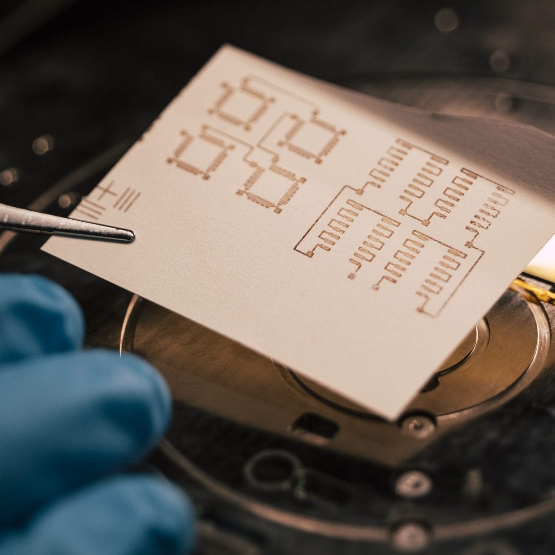
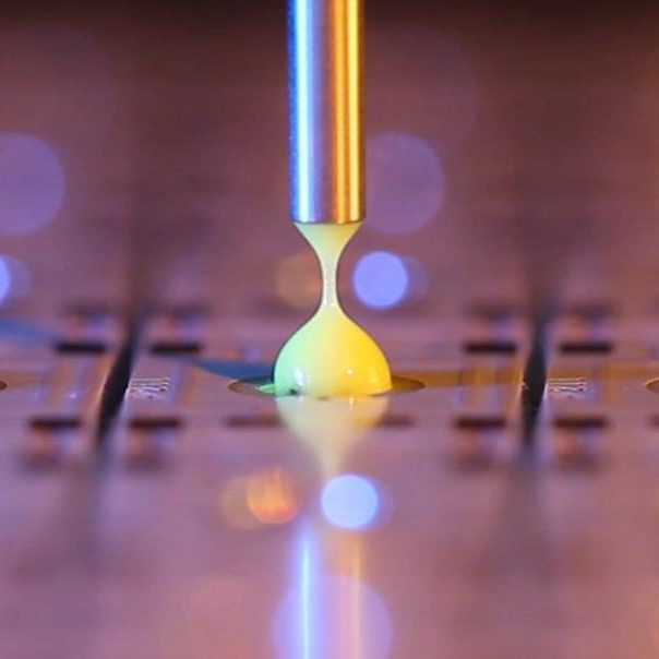
Skalierbare und digitale Druckverfahren (inkl. 3D-Druck von Elektronik) zur Generativen Fertigung funktionaler Komponenten
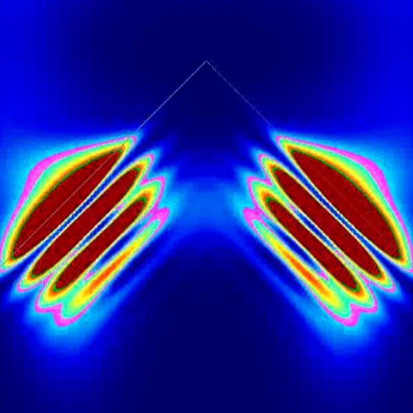
Gesamtkonzepte für Design, Simulation, Optimierung und Prototyping von optischen Komponenten für maßgeschneiderte Lichtlösungen
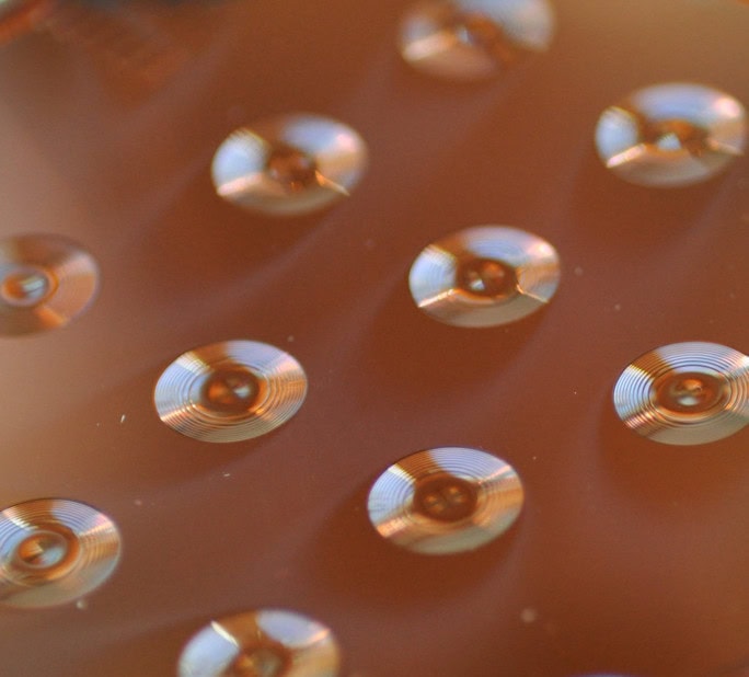
Hochauflösende 3D-Strukturierung mittels Zwei-Photonen-Lithografie sowie stufenlose 2.5D-Strukturierung mittels maskenloser Graustufen-Laserlithografie oder Laserablation und Elektronenstrahllithografie