SiTaSol: Sustainable Solar Cells
Application relevant validation of c-Si (crystalline silicon) based tandem solar cell processes with 30 % efficiency target
Crystalline silicon wafer solar cells have been dominating the photovoltaic market so far due to the availability and stability of c-Si and the decades of Si technology development.
However, without new ways to improve the conversion efficiencies further significant cost reductions will be difficult and the c-Si technology will not be able to maintain its dominant role. In particular, with respect to conversion efficiency Si solar cells today already are close to their technologically limit. Compared to that until today III-V multijunction solar cells did already show that the current generation can almost be doubled at the same solar cell size.
In SiTaSol we address exactly this topic and want to increase conversion efficiencies of c-Si solar cells to 30 % by combining it with III-V top absorbers.
Such a tandem solar cell, due to its high efficiency, will provide significant potential savings with respect to consumption of resources and ecological footprint and thus offers clear advantages compared to today’s products. Furthermore, the combined III-V/Si solar cell will allow for a drop-in-replacement of today’s Si flat plate terrestrial PV. Yet, in order to achieve competitiveness for this technology it is necessary to lower the production costs for the novel solar cell materials by a factor of 100. It is the intention of SiTaSol to evaluate industrially applicable processes that can meet this challenging cost target and to proof that such a solar cells can be produced in large scale. In order to achieve that only a few micrometer thick III-V layers will either be grown directly on a Si substrate or will be transferred from a III-V substrate by a particular lift-off process.
During the first part of the project we will focus on both approaches in order to focus on the more promising solution afterwards.
Another emphasis is set on the development of a cost efficient deposition process for III-V layers aiming for an efficient use of precursor gases, enhanced waste treatment, recycling of metals as well as on the development of processes for lift-off and transfer of III-V epitaxial layers to the Si solar cell.

III-V/Si tandem-solarcells are either grown directly on a Si substrate or bonded to Si by a transparent conductive layer (TCO).
It is the final goal in SiTaSol to produce high performance solar cell devices in an industrial relevant environment featuring conversion efficiencies of 30% and thereby applying the newly developed cost efficient production processes.
In addition to the technological developments, in SiTaSol a thorough life cycle analysis is conducted where material and energy flows will be analyzed as well as possible hazards due to the usage of toxic materials. The development of new photovoltaic technologies will adapt to high environmental standards right from the beginning.
The project SiTaSol brings together some of the most well-known European partners in the field of Si PV and III-V compound semiconductors. Apart from the progress in the field of photovoltaics, SiTaSol thereby will support the competitiveness of the European industry by providing innovative solutions for lowering manufacturing costs of III-V materials which are essential in today’s electronic products including laptops, photonic sensors and light emitting diodes.
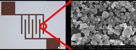
Printed nanometal inks are deposited on the surface of the III-V material and analyzed with respect to their morphology, conductivity and material composition.
MATERIALS has many years of excellent experience in research and development of novel photovoltaic technologies on both single cell as well as on module level. In particular, in SiTaSol MATERIALS provides its expertise on the one hand with the application of laser production processes and on the deposition of metallic back contacts. The detailed experience at the institute thus enables the development of industrially applicable cost efficient processes for a large-scale lift-off of III-V layers as well as for an efficient and resource conserving metallization of solar cell devices.
- nano- and picosecond-laser- structuring
- PVD processes
- inkjet-processing of nanometal-inks
- material development featuring well adjusted properties tuned for the specific application
- surface modification for the desired applications
- process development
- Surface and material characterization (XPS, UPS, electron microscopy)
- electrical layer and device characterization