Organic transistors with short chanellengths
For a given effective charge carrier mobility, the switching speed of organic thin-film transistors (OTFTs) is determined by two factors:
- the channel length, i.e. the distance between the channel electrodes (source and drain)
- the parasitic gate capacitance, which is mainly determined by the area of overlap between channel electrodes and gate electrode
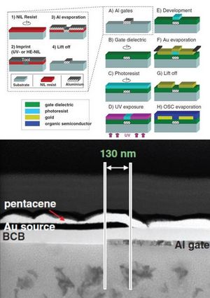
The smaller channel length and overlap are, the faster an OTFT can get. In order to minimise both parameters in one process we have developed a self-aligned process for OTFTs, where a nanoimprinting process (NanoImprint Lithography, NIL) is combined with a back-substrate exposure step. In a first step a high-definition gate electrode is fabricated by means of NIL, which serves as an intrinsic photomask in a further step for the photolithographic definition of the channel electrodes, where UV-exposure is carried out through the transparent substrate. With that short channel OTFTs with minimised electrode overlap are realized. This process has been successfully employed for the fabrication of OTFT-based flexible active-matrix addressing backplanes for Liquid-Crystal-Displays (LCDs) in a large European project (POLARIC).
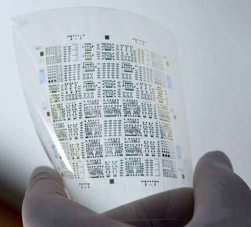
In a modification of this process the gate electrode is defined by contact photolithography instead of NIL. Here, channel lengths are not entirely that short, yet we can pattern active areas of up to 6” on a single flexible substrate. In this way, analog circuits of some 10s of OTFTs and a footprint of a fraction of a cm² were realised, as e.g. a 10kHz clocked comparator.
Minimizing Source-Drain to Gate overlap by self-alignment